


XC7K325
Model
AV7K300Ean
6971390278499Price
$ 1320
Meet the requirements of users for various PCIe high-speed data transmission, video image processing and industrial control

Supporting Verilog HDL Demos and Docuemnts.All Doucments Saved in Dropbox, after buy the board, email to get it.
00. vivado 2017.4 Installation
01. LED water lamp experiment and simulation in vivado
02. Key detection experiment in Vivado
03. PLL Experiment in Vivado
04. Serial port Transmitting and Receiving experiment
05. Key debounce experiment
06. LM75 Temperature Test Experiment
07. SD Card Read and Write Experiment
08. SDI LCD Test Experiment
09. DDR3 Read Write and Simulation Experiment
10. Recording and playback Experiment of AN831 Module
11. SD Card Music Player Experiment
12. Character Display Experiment
13. SD Card Read BMP Picture Display Experiment
14. OV5640 Camera Display Experiment
15. SOBEL Edge Detection Experiment
16. AD7606 Waveform Display Experiment
17. ADDA Testing Experiment
18. AD9767 Waveform Display Experiment-Dual channel Sine Wave Experiment
19. AD9767 Waveform Display Experiment-Dual channel Triangle Wave Experiment
20. GTX Fiber Optic Communication IBERT Testing Experiment
21. GTX Fiber Optic Data Communication Experiment
22. Video Image GTX Fiber Optic Communication Testing Experiment
23. PCIe Speed Test Experiment
24. PCIe SDI Input Experiment
25. PCIe SDI Output Experiment
26. PCIe xdma Interface Experiment Testing Experiment
FPGA Board
AN9767 Collection Package
AN706 Collection Package
AN9238 Collection Package
Video Package
Luxury Package
FPGA Board
●
●
●
●
●
●
Downloader Cable USB
●
●
●
●
●
●
AN9767
●
●
AN706
●
●
AN9238
●
●
Binocular Camera
●
●
4.3-inch LCD
●
●
Supporting Modules in the Package, Click to Learn More


*Learn More about the Core Board, Click to View >

FPGA Chip
XC7K325T-2FFG900I
PCIe Gen2
X8
Logic Cells
326,080
Transceiver
16X 12.5Gb/s max
Look Up Tables (LUTs)
50,950
CLB Flip-Flops
407,600
Block RAM
16,020Kb
DSP
840
Temperature class
Industrial Grade, -40℃-85℃
XADC
1× 12bit, 1Mbps AD
Speed Grades
-2
DDR3
4x 512MB DDR3, 64 bit Bus, Data Rate 1600Mbps
QSPI Flash
128Mbit, Used as FPGA User Data Storage
Crystal Oscillator
200MHz Provide Stable Clock Source for the System
125MHz Provide Stable Clock Source Input for the GTX transceiver
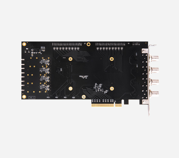
PCIe 2.0 x 8
Used for PCIe communication with computer motherboard Single Channel Communication Rate can be up to 8Gbps
SFP
4 SFP Interfaces, the Speed of Each Channel is up to 10Gb/s
JTAG
Standard JTAG Port for Debug and Download of FPGA Program
3G-SDI
HD 3G-SDI Interfaces, Support Data Input / Output in Different Formats ( HDcctv 1.0, HD-SDI ( ST292 ), 3G-SDI ( ST-424 ) and SD-SDI ( ST259 )
JTAG
Standard JTAG Port for Debug and Download of FPGA Program
USB Uart
Used for Serial Communication with PC or External Devices
SD Card Slot
1 Micro SD Card Slot, Support the SD Mode and SPI Mode
LED
4 User LEDs
Key
4 User Keys
40-Pin Expansion Ports
Reserved 40-Pin Expansion Ports ( 0.1 inch Pitch ), Can be Connect with Various ALINX Modules ( Binocular Camera Module, TFT LCD Screen, Camera, AD / DA and Other Modules )
Voltage Input
+12V DC
Current Input
Max. Current 3A
FPGA Board
1
DC Fan ( Fixed on the Board )
1
Mini USB Cable
1
USB Downloader Cable
1
12V Power Adapter
1
PCIe Fence
1
Size Dimension
Core Board 3.15 inch x 2.36 inch, Carrier Board 8.46 inch x 4.37 inch
Number of Layers
8-Layer Core Board PCB, 6-Layer Carrier Board PCB Reserve Independent Power Layer and GND Layer

Core Board Size Dimension

Carrier Board Size Dimension
SFP Communication, PCIe Aaccelerator Video Processing, High-Data Transmission
Core Board + Carrier Board, Customers Can Directly Use the Core Board in their Design.
Rich Interfaces in the Carrier board. PCIe x8, 4 SFP, USB Uart, SD Card Slot 2X 3G-SDI Output, Supports 1080P@60Hz Output 2x 3G-SDI Input, Support 1080P@60Hz Input Apply to SDI Video Image Processing
Binocular Camera Moulde for SFP Video Transmission


The FPGA Development Board Collects the Video Image through the Camera Module, Transmits it to Another FPGA Development Board through SPF, and displays to the PC Monitor through the SDI interface.

SFP 10G Transceiver Communication Eye Diagram
Verify PCIE Solution Speed up PCIE Product Development

Collect the Video Signal through the SDI Input Interface Upload it to the Computer Through the PCIE Interface, and Display the Video Image in Real Time

The Host Computer Grabs the Computer Desktop, and Transmits it to the FPGA through the PCIE Interface. The FPGA Outputs through the SDI Interface, The Monitor Displays in Real Time
Meet various PCIe high-speed data transmission and video image processing

Dual Lens Camera Module On-Board Demo

Binocular Camera Module AN5642 for Video Capture Display on the Monitor through the SDI interface to Realize Binocular Display Simultaneously
AN9767 / AN706 Module On-Board Demo

*The Signal Source Output Signal is Connected to the AN9767 Module,
and the Waveform Signal is Displayed through the Oscilloscope
*The Signal Source Output Signal is Connected to the AN706 Module
Run the System to Draw the Waveform Data, and is Displayed to the Monitor through the SDI Interface of the FPGA Development Board
The warranty period of all products sold is 12 months, of which FPGA chips and LCD screens are wearing parts and are not covered by the warranty. All accessories and gifts are not covered under warranty.
Links:


Alinx Electronic Technology (Shanghai) Co., Ltd. 滬ICP備13046728號


