
XC7Z021
Model
AX7021 / AX7021BEan
6971390270622Price
$ 560Notice for purchase:
This series of development boards include AX7021 and AX7021B.
Only the Ethernet interface chips of the expansion board are different, and the functions are the same.
The two models will be delivered randomly according to the inventory, please distinguish them according to the QR code label.
Video Transmission Processing, Industrial Control 8GB eMMC, 1GB DDR3, HDMI Output

AX7021 Supporting Verilog HDL Demos and Docuemnts. All Doucments Saved in Dropbox, after buy the board, email to get it.
Course S1 Basic Tutorial
01: Software Package Introduction and FPGA Board Inspection
02: Introduction to ZYNQ
03: Vivado development environment
04: PL's "Hello World" LED experiment
05: HDMI output experiment
06: Experience ARM, bare metal output "Hello World"
07: PS lights up the LED lights of the PL
08: PS timer interrupt experiment
09: PL button interrupt experiment
10: Ethernet Experiment (LWIP)
11: Custom IP experiment
12: Use VDMA to drive HDMI display
13: Curing procedure
14: Install virtual machine and Ubuntu system
15: Ubuntu installs the Vivado software for Linux
16: Petalinux tool installation
17: NFS service software installation
18: Customizing Linux with Petalinux
19: Develop Linux programs using the SDK
20: GPIO experiment under Linux
21: HDMI display under Petalinux
22: Use the Debian 8 desktop system
23: Making QSPIFlash boot Linux
24: Petalinux tool installation
25: QSPI and EMMC boot Linux
Course S2 SDK Application Tutorial
01: PS side MIO operation—light up the LED Light
02: PS side MIO operation—Key interrupt
03: PS side UART read and write control
04: PL read and write PS DDR data
05: Realize PS and PL data interaction through BRAM
06: Use of dual core AMP
07: Use of Free RTOS under ZYNQ
08: DMA loop test
09: Use of DMA-DAC waveform generator ( AN108 )
10: Use of DMA-ADC oscilloscope ( AN108 )
11: Use of DMA-ADC oscilloscope ( AN9238 )
12: Use of DMA-ADC oscilloscope ( AN706 )
13: Use of the SG DMA based on ADC module ( AN108 )
14: Use the SG DMA based on DAC module ( AN9767 )
15: OV5640 camera acquisition display (1)
16: OV5640 camera acquisition display (2)
17: Binocular camera Ethernet transmission
18: Use of 7 inch LCD module
19: Use of 7-inch touch screen disaply
20: SD card read and write operation BMP picture display
21: SD card read and write operation camera capture
22: Ethernet Transmission ADC Acquisition Based on AN108 Module
23: Ethernet Transmission ADC Acquisition Based on AN706 Module ( AN9238 )
24: Ethernet Transmission-ADC Acquisition Based on AN706 Module
25: Remote update QSPI Flash based on UDP/TCP
Course S3 HSL Application Tutorial
01: Getting to Know HLS
02: Status Indicator LED
03: Floating Point Coprocessing
04: Video Color Bar
05: Video Frame Buffer Read and Write Management
06: Image Scaling Overlay
07: Character Overlay
08: Image Contrast Adjustment
09: Auto Focus
10: Edge Detection
11: Corner Detection
12: Fast Fourier Transform
Course S4 Linux Application Tutorial
01: QT application on ZYNQ
02: OpenCV Application( USB Camera Display )
03: Binocular Camera Module OpenCV Display
04: Touch screen module application
05: AXI DMA Read and Write Test
06: DMA-based ADC Waveform Display ( AN9238 )
07: DMA-based ADC Waveform Display ( AN706 )
08: Autorun petalinux application
09: Appendix - Linux Common Commands
FPGA Board
AN9767 Collection Package
AN706 Collection Package
AN9238 Collection Package
Video Package
Luxury Package
FPGA Board
●
●
●
●
●
●
AN9767
●
●
AN706
●
●
AN9238
●
●
Binocular Camera
●
●
7-inch LCD
●
●
Supporting Modules in the Package, Click to Learn More


*Learn More about the Core Board,Click to View>>

FPGA Board
AX7021
FPGA Chip
XC7Z020-2CLG484I
Kernel
Dual-Core ARM Cortex-A9, Main Frequency 767MHz
Speed Grades
-2
Working Temperature
-40°c~85°c
Look Up Tables ( LUTs )
53,200
CLB Flip-Flops
106,400
eMMC FLASH
8GB
PS MIOs ( ARM )
39
LVDS
48
RAM
DDR3 1GB, Data Rate 1066Mbps
Chip Level
Industrial Grade
Logic Cells
85K
Multiplier
220
Block RAM
4.9Mb
QSPI FLASH
256MBit
PL IOs ( FPGA )
198
Voltage Adjustable IOs
100
DDR3
Two 512MB DDR3, 32bit Bus, Data Rate 1066Mbps
QSPI Flash
256Mbit, Used as FPGA User Data Storage
EMMC Flash
8GB, Used as a Large-Capacity Storage Device in the ZYNQ System
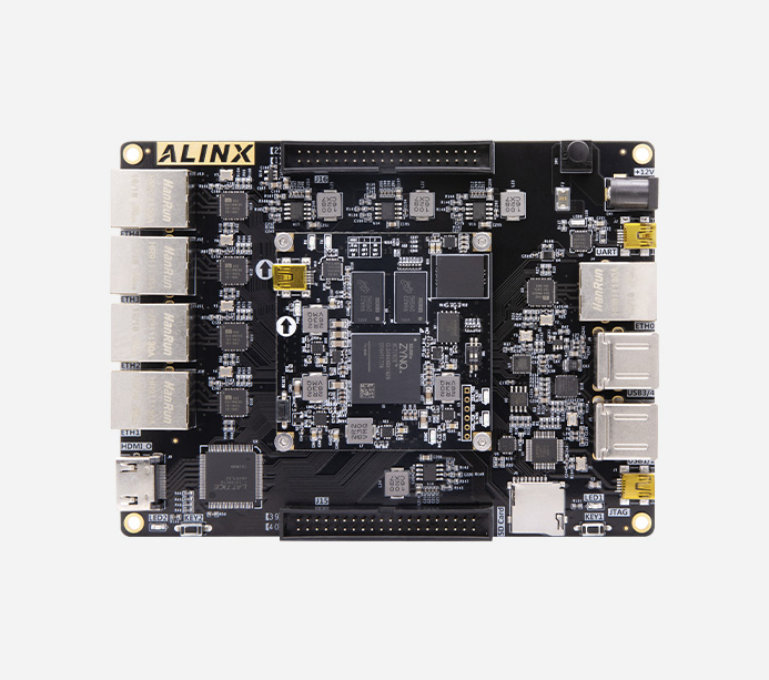
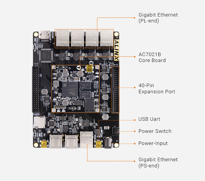
Gigabit Ethernet
5×10/100M/1000M Ethernet RJ-45 Interfaces for Ethernet Data Exchange
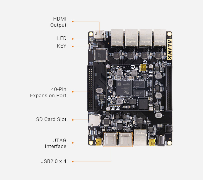
JTAG
1 USB JTAG Interface Onboard, No Need to Purchase Xilinx Downloader
HDMI Output
HDMI Video Output Interface, Support up to 1080P@60Hz Output, Support 3D Output
USB 2.0 x 4
Used for Connect USB Peripherals such as Mouse, Keyboard and U-Disk
USB Uart
Used for Data Exchange with Computers and Other Network Equipment
Crystal Oscillator
33.333Mhz Provide Stable Clock Source for the PS System
50MHz Provide Extra Clock for PL Logic
TF Card Slot
Insert Micro SD TF Card, Store Operating System Image and File System
LED
2 LED lights, 1 Controlled by PS, 1 Controlled by PL
kEYs
2 Keys and 1 Reset Key, 1 PS Control key, 1 PL Control Key
40-Pin Expansion Ports
Two 40-Pin Expansion Ports (0.1 inch Pitch), Can be Connect with Various ALINX Modules (Binocular Camera Module, TFT LCD Screen, Camera, AD/DA and Other Modules).
Voltage Input
+12V
Current Input
Max. Current 2A
FPGA Board
1
TF Card
1
Mini USB Cable
2
Transparent Protection Board
1
12V Power Adapter
1
Card Reader
1
Size Dimension
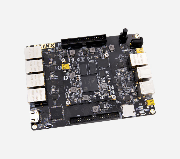
Core Board 2.36 inch x 2.36 inch, Carrier Board 7.40 inch x 4.17 inch
Number of Layers
10-Lay Core Board PCB, 4-Layer Carrier Board PCB

Data Processing and Storage Video Transmission Processing Industrial Control
5 Network Ports Simultaneously Drive Successfully

Intelligent Identification, Medical Security, Vehicle Digital, Industrial Control, Smart Grid

The Binocular Camera Module AN5642 for Video Capture, and Displays it on the Monitor through the HDMI Interface of the ZYNQ Development Board. The ZYNQ Development Board Runs the Linux Operating System, and the Video Data is Displayed Using QT to Realize Binocular Display Simultaneously.
AN9767 / AN706 Module On-Board Demo

*The Signal Source Output Signal is Connected to the AN9767 Module, and the Waveform Signal is Displayed through the Oscilloscope
*The Signal Source Output Signal is Connected to the AN706 Module,
Run the System to Draw the Waveform Data, and is Displayed to the Monitor through the HDMI Interface of the FPGA Development Board
The warranty period of all products sold is 12 months, of which FPGA chips and LCD screens are wearing parts and are not covered by the warranty. All accessories and gifts are not covered under warranty.
Links:


Alinx Electronic Technology (Shanghai) Co., Ltd. 滬ICP備13046728號


