


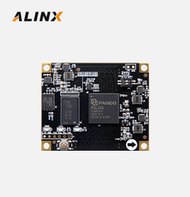
PGL50H
Model
AXPGL50HEan
6971390271629Price
$ 300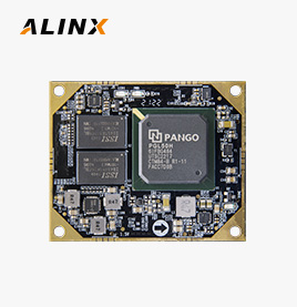
PANGOMICRO Logos PGL50H FPGA SoM Core Board Industrial Grade DDR3 P50
PANGOMICRO Logos2 PG2L100H SoM Core Board Industrial Grade P100
PANGOMICRO Titan-2 PG2T390 FPGA Development Board Evaluation Boards & Kits PCIe Optical Communication DDR4 FMC AXP390
PANGOMICRO Logos PGL22G FPGA SoM Core Board P22
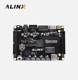
PANGOMICRO Logos PGL12G FPGA Development Board Evaluation Boards & Kits HDMI Output Video Image Processing PGL12G
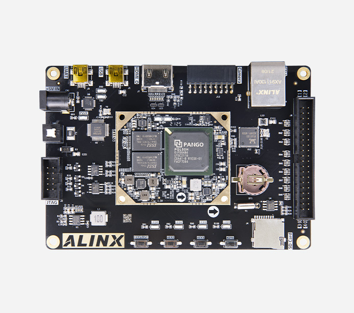
HDMI output interface, USB, Ethernet, camera interface, JTAG debugging interface, 1-way 40PIN extension port, RTC clock, etc. meet the requirements of video image processing and industrial control

Supporting Verilog HDL Demos and Docuemnts,All Doucments Saved in Dropbox, after buy the board, email to get it.
01. Pango Design Suite 2021.1-sp7 Installation
02. LED water lamp experiment and simulation
03. Key detection experiment
04. PLL phase-locked loop output test
05. Serial port Transmitting and Receiving experiment
06. Key debounce experiment
07. I2C Interface EEPROM Experiment
08. SD Card Read and Write Experiment
09. HDMI Programming Output Experiment
10. 4.3 inch screen color bar output
11. 7-inch screen color bar output
12. SDRAM read and write data testing
13. AN831 Recording and Playback
14. SD Card Music Player Experiment
15. Character HDMI display
16. Character 4.3 inch screen display
17. Character 7-inch screen display
18. SD card image HDMI display
19. SD card image 4.3 inch LCD display
20. SD card image displayed on a 7-inch screen
21. AN5640 camera captures HDMI display
22. AN5640 camera captures a 4.3 inch screen display
23. AN5640 camera captures 7-inch screen display
24. AN5642 binocular camera captures HDMI display
25. Camera edge detection HDMI display routine
26. Camera edge detection 4.3 inch screen display routine
27. Camera edge detection 7-inch screen display routine
28. AD9238 waveform display routine
29. AD7606 waveform display routine
30. ADDA Test Routine
31. AD9767 Dual Channel Sine Wave Generation Routine
32. AD9767 Dual Channel Triangular Wave Generation Routine
33. RTC Clock Experiment
34. Gigabit Ethernet Transmission Experiment
35. AD 9280 Ethernet transmission routine
36. AD7606 Ethernet Transmission Routine
37. AD9280 Ethernet Transmission Routine
38. AN5640 Gigabit Ethernet for video transmission
39. AN5642 Gigabit Ethernet for video transmission
40. USB bidirectional speed measurement routine
AN108 Collection Package
AN9767Collection Package
AN706 Collection Package
AN9238 Collection Package
Binocular Camera Package
Single camera video package
Luxury Package
FPGA Board
●
●
●
●
●
●
●
USB Downloader
●
●
●
●
●
●
●
AN108
●
●
AN9767
●
●
AN706
●
●
AN9238
●
●
AN5642
●
●
AN5640
●
●
4.3-Inch LCD
●
●
Supporting Modules in the Package, Click to Learn More


Learn More about the Core Board, Click to View>>

FPGA Chip
PGL50H-6IFBG484
Chip level
Chip speed level -6, chip temperature level industrial grade
Flip-Flop ( FF )
64200
LUT5
42800 ( LUT5=1.2LUT4 )
DRM ( 18Kbits )
134
APM Unit ( Multiplier )
84
PCIe Gen2 x4
1
HSST
4x 6.375Gb/s max
PLL
5
AES
1
DDR3
2x 512MB, 1GB in total, 32bit bus for data caching
QSPI Flash
128Mbit QSPI FLASH, Used for FPGA Configuration File and User Data Storage
Crystal Oscillator
1x 125MHz active differential crystal oscillator, providing reference input clock for the internal HSST module of FPGA
50 Mhz Provide Reference Input Clock for FPGA
HDMI Output
1 channel HDMI output, providing video output interfaces in different formats for the development board
Gigabit Ethernet
One 10 / 100M / 1000M Ethernet with RJ-45 Interfaces for Data Exchange
USB
1-way USB2.0 interface for high-speed communication between development board and PC using USB2.0
Uart
1-way Uart to USB interface for communication with computers, facilitating user debugging
EEPROM
1 EEPROM 24LC04 with IIC interface
CMOS
18-pin camera interface that can connect to a 5 million OV5640 camera
RTC
One way RTC Real-time clock, equipped with battery holder, and the battery model is CR1220 (self purchased)
JTAG
10-pin 2.54mm standard JTAG port for downloading and debugging FPGA programs
SD Card Slot
1 Micro SD Card Slot, Support the SPI Mode
LED
5 User LEDs (1 LED in the Core Board, 4 LEDs in the Carrier Board )
KEYs
4
40-Pin Expansion Ports
1x 40-pin 2.54mm spacing expansion port, capable of connecting various modules ( binocular camera, LCD screen, high-speed AD module, etc ) The expansion port includes 1x 5V power supply, 2x 3.3V power supplies, 3 ground supplies, and 34 IO ports
power supply
5V, 2A
FPGA Board
1
USB Downloader Cable
1 Set
Mini USB Cable
1
5V power supply
1
12V Power Adapter
1
Size Dimension
130mm x 90mm
Number of Layers
14-Layer Core Board PCB, 4-Layer Carrier Board PCB


The Logos series FPGA adopts a 40nm CMOS process and a new LUT5 structure, integrating rich on-chip resources such as RAM, DSP, ADC, Serdes, DDR3, and IO interfaces. It has low power consumption, low cost, and rich functions, providing customers with cost-effective solutions. It is widely used in industrial control, communication, consumer fields, and other fields, making it an ideal choice for customers in large-scale, cost sensitive projects.

The Binocular Camera Module AN5642 for Video Capture Displays it on the Monitor through the HDMI Interface and Realize Binocular Display Simultaneously
AN9767 / AN706 Module On-Board Demo

*The Signal Source Output Signal is Connected to the AN9767 Module, and the Waveform Signal is Displayed through the Oscilloscope
*The Signal Source Output Signal is Connected to the AN706 Module, Run the System to Draw the Waveform Data, and is Displayed to the Monitor through the HDMI Interface of the FPGA Development Board

The warranty period of all products sold is 12 months, of which FPGA chips and LCD screens are wearing parts and are not covered by the warranty. All accessories and gifts are not covered under warranty.
Links:


Alinx Electronic Technology (Shanghai) Co., Ltd. 滬ICP備13046728號


