XCZU47DR
Model
ACRF47Price
$ 11227RFSOM integrates hardware and software to help you provide a prototype of a high-performance wireless receiver system and perform air signal acquisition and analysis. In addition, RFSOM adopts a RF direct sampling structure with eight independent transmitter and receiver channels. It integrates a programmable Xilinx RFSoC FPGA minimum system, supports software defined radio development architecture, has large bandwidth and large-scale computing processing capabilities, and can be used for wireless communication prototype verification, spectrum monitoring, signal intelligence, and broadband acquisition and recording applications. The RFSOM is also equipped with a 19.2 MHz constant temperature crystal oscillator (OCXO) reference clock, which improves frequency accuracy and synchronization.

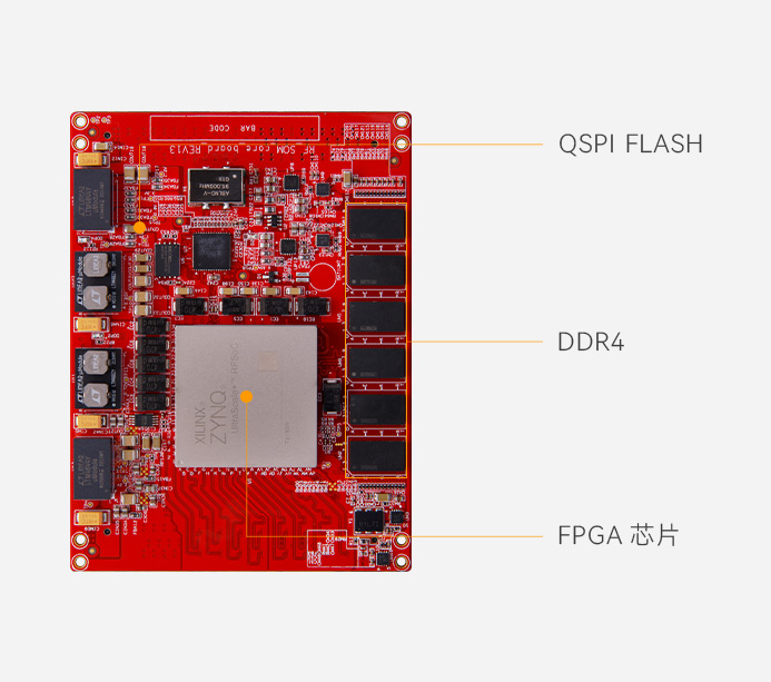
PS DDR4
PL DDR4
QSPI FLASH
8 GTY
8 14bit ADC
8 14bit DAC

With Zynq? RFSoC, wireless infrastructure manufacturers can achieve previously unattainable footprint and power reduction, critical to Massive MIMO deployment.
Zynq UltraScale+? RFSoC enables cable access multi-service operators (MSOs) to move PHY layer processing closer to home with remote PHY nodes, increasing network capacity.


As a single-chip TRX solution for scalable, multi-function, phased array radar, the Zynq UltraScale+ RFSoC enables low latency transmit and receive for optimal response time in early warning scenarios.
Designers can build high-speed multi-function instruments for signal generation and signal analysis by using direct RF-sampling, highly flexible, reconfigurable logic, and software programmability in Zynq UltraScale+ RFSoC.


Designers can build high-speed multi-function instruments for signal generation and signal analysis by using direct RF-sampling, highly flexible, reconfigurable logic, and software programmability in Zynq UltraScale+ RFSoC.
The FPGA resources of the programmable logic portion of Xilinx Zynq UltraScale+FPGA can provide high throughput digital signal processing (DSP) and IP cores, such as digital up/down conversion (DUC/DDC) cores. It is easier to achieve FPGA acceleration through software defined radio development architecture, application programming interfaces, and FPGA infrastructure. This helps you get up and running quickly so you can focus on value-added IP. The FPGA system used for commonly used functions such as Fast Fourier Transform (FFT) and Finite Impulse Response (FIR) filters is a good starting point. Then, you can use the preferred Hardware Description Language (HDL) to add your IP blocks to the modular architecture. In addition to the FPGA architecture of the system, Xilinx UltraScale+RFSoC is also equipped with four onboard application processing units (APUs) and two real-time processing units (RPUs), suitable for applications that require independent operation of onboard embedded operating systems

ACRF47 can support full differential extraction of AD/DA channels, and users can define RF conditioning circuits according to their needs, supporting DC and AC coupling, as well as PA and LNA amplifier conditioning circuits. It can also support optional RF front-end, including Lo frequency converters, duplexers, PA, LNA, etc.


*Corresponding development board AXRF47, click to learn more>>
· Intgrateed Device of ZU47DR RF System on Chip (RFSoC)
· Equipped with built-in digital up and down conversion and interpolation extraction functions
· Supports 8-way transmission and 8-way reception
Simulate RFMC connectors
1. ADC/DAC fully differential lead out, supporting DC or AC coupling
2. VCM export supports setting common mode level
Digital RFMC connector
1. GTY export, supporting PCIE4.0X8 rate transmission
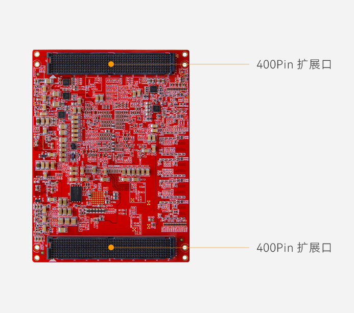
2. MIO export, supporting expansion of Ethernet, USB and other peripheral interfaces, supporting peripheral level
3. GTR export, supporting expansion of storage interfaces such as Sata/PCIE hard drives, and supporting external device levels
4. HD IO output, supporting peripheral device level
CACHE
1. PL DDR4 32bit single channel DDR4 cache supports 2600MHz, 2GB capacity
2. PS DDR4 64bit single channel DDR4 cache supports 2133MHz and 4GB capacity
3. QSPI flash, 1GB capacity
Debug Interface
1. JTAG lead out
2. Reset signal lead out
·Built in LMK04828 dedicated clock circuit
·Integrated 19.2MHz OCXO
·External clock synchronization
·Trigger synchronization
·SYSREF synchronization
·5V single power supply
·Heat sink embedded fan
·Typical power consumption, running 50% logic,8TX&8RX,TBD Watt
·API supports real-time bandwidth of 30.72/61.44/122.88/245.76/491.52/983.04MHz (maximum support for 2.5GHz bandwidth)
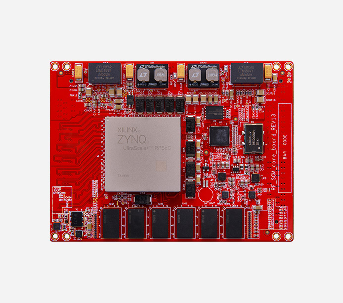
Core board
ACRF47
FPGA model
XCZU47DR-2FFVE1156I
kernel CPU
Quad-core ARM Cortex-A53, MPCore
Dual-core ARM Cortex-R5F, MPCore
Memory
PS DDR4,4GB
PL DDR4,2GB
14 bit 5.0GSPS RF-ADC
8
14 bit 9.85GSPS RF-DAC
8
Decimation/ interpolation
1x, 2x, 3x, 4x, 5x, 6x, 8x, 10x, 12x, 16x, 20x, 24x, 40x
GTY / GTR
PL GTY8 / PS GTR4
System Logic Cell
930K
CLB LUTs
425K
Max.Dist.RAM
13.0Mb
Total Block RAM
38.0Mb
UltraRAM
22.5Mb
DSP Slices
4272
PCIe Gen4 x8
1
EVM emission: Under typical frequency bands, EVM is better than 1%

Flatness: Output flatness at 1GHz bandwidth

phase noise

FPGA Core board
1
Size
115mm x 85mm
Stacking quantity
Core board 14 layer PCB board design, with reserved independent power layer and GND layer

Dimensional diagram of core board structure

The warranty period of all products sold is 12 months, of which FPGA chips and LCD screens are wearing parts and are not covered by the warranty. All accessories and gifts are not covered under warranty.